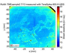
Fig. 1: High-resolution sheet resistance image acquired at a metal mesh covered glass wafer fabricated through Rolith, Inc..
Following recent economic predictions the market for transparent conductor technologies excluding the yet standard material indium tin oxide (ITO) will see a significant increase from $206 million in 2013 to $4 billion by 2020 [1]. The applications requiring transparent conductors are manifold ranging from touch sensors, displays, lighting, thin-film solar cells to smart windows and others. Since ITO has deficits in terms of cost, mechanical flexibility and sheet resistance many companies like Atmel, Fujifilm, Cambrios, Rolith, Unipixel as well as research institutes are working on (and have already brought to market) alternative solutions such as graphene layers, silver nanowire dispersions or metal mesh nanostructures. Especially the latter approach appears to be very promising by offering superior conductivity, transparency and flexibility.However, the efficient development of non-ITO technologies also relies on the availability of powerful analysis tools. High-resolution measurements of sheet resistance distributions on large-scale areas, for example, have been a major problem so far and emerging transparent conductor technologies have even raised the analytic requirements. Metal mesh structures – typically consisting of sub-µm-wide wires – require time-consuming and destructive application of sufficiently large contact pad structures to enable contact based measurements. Existing contactless methods on the other hand (e.g. Eddy current based systems) are limited to only mm-scale spatial resolution – too low to visualize any local defects or inhomogeneity.
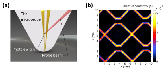
A new measurement tool recently developed by AMO GmbH, Germany, employing THz radiation in combination with the highly-resolving contactless microprobes (TeraSpike) [2] represents an important step towards the elimination of this lack. Offering quantitative sheet resistance measurements with up to 10 µm resolution the system has been applied recently to structured graphene layers from the Korean manufacturer Samsung Techwin [3]. Now the system has been used to demonstrate the prime performance of the metal mesh technology available from the Californian start-up company Rolith. Metal structures were fabricated in the form of submicron-width nanowires completely invisible to the human eye, lithographically placed in a regular 2-dimentional grid pattern with a period of tens of microns and thickness of a few hundreds of nanometers [4].
The highly detailed sheet resistance image (Fig. 1) acquired with the new THz microprobe scanner system from AMO using a scanning speed of 5 ms/Pixel reveals the low resistivity (<14 Ohm/☐) of the metal mesh fabricated by Rolith. Together with a transparency of >94% and very low haze (~2%) the manufacturer now considers his “technology above all major competition for ITO-alternative technologies” [4].
[1] http://touchdisplayresearch.com/?page_id=358
[2] https://www.amo.de/thz_tip.0.html?&L=1&L=2
Related articles
- Rolith Demonstrates superior Performance of ITO-alternative Transparent Metal Grid Electrodes Fabricated Using Proprietary Nanolithography Technology (nanowerk.com)
- The metal coating that makes iPhones touch sensitive is running out (gigaom.com)
- Global Transparent Conductive Films (TCF) Market will be over $1.63 billion in 2013: Worldwide Industry Forecasts, Technologies, Players 2013-2023 : MarketResearchReports.Biz (virtual-strategy.com)
- Fujifilm reinforces the production facilities for its touch-panel sensor film “EXCLEAR” (Fujifilm.com)

